By Dr Karl Bitzer, head of product management at DELO Industrial Adhesives
With ever increasing power electronics and the demand for more efficiency in production, miniaturisation has become a global trend. The adhesive industry has responded to that trend with numerous new developments that are becoming increasingly common in the market.
Epoxy resins are used almost exclusively to provide resistance to increasing thermal, mechanical and chemical influences. However, epoxy resins are not all the same. For the highest reliability requirements, for example, epoxy resins are used with very specific hardeners, which ensure particularly tight crosslinking of the adhesive molecules. This makes potting compounds and encapsulants highly resistant to temperature and media, allowing them to be used permanently in hot transmission fluid or aggressive media.
The temperature requirements for electronic components have recently increased in many areas. This is true for automotive sensors or oil drilling equipment, for example. It is also especially true for power electronics since ever-increasing currents flow through increasingly smaller components, resulting in an increase of trapped heat.
Due to these developments, the service temperature range of previous highly reliable encapsulants of 180°C is not always sufficient. However, newly developed products have been able to extend this limit upward by up to 70°C and can be used at temperatures ranging from -65°C to 250°C.
While still featuring high media resistance, these high temperature encapsulants and potting compounds provide universal adhesion and a high-level of strength. Despite the large number of fillers, they also provide solid processing properties and good flow behaviour. Even after 500 hours of storage at 250°C they provide a tensile strength of 50 MPa. They also combine high temperature resistance with high bond strength at temperatures of over 200°C. After storage for 500 hours at 250°C, the compression shear strength on ceramic measured at 220°C is 8 MPa; this corresponds to 800N/cm².
Whether at 180°C or 250°C adhesives, potting compounds and encapsulants for the high-end sector have so far only been available as purely heat curing products, since the special hardeners must be melted at temperatures of at least 100°C before they can react with the resin.
Heat curing is also required for dual curing compounds that have recently become available. However, these hybrid products additionally allow a light fixation process to take place initially, enabling greater bonding accuracy, a defined fillet and easier handling of the fixed components.
What’s more, in the case of glob top encapsulation, which is a round encapsulation for chip protection, the process forms a skin and freezes its shape, preventing the compound from flowing during heat curing. This means that a defined glob top encapsulation is possible, even if miniaturisation makes space tight on the circuit board. Compared to the alternative ‘dam & fill’ method, light fixation makes it possible to save one process step.
In a two stage curing process, the adhesive is first light cured in 1 to 5 seconds, depending on the LED lamp’s intensity. On the typical FR4 PCB material, it achieves a die shear strength of more than 1N. The adhesive then develops its full strength of 50 MPa on FR4 after heat curing for 30 minutes at 150°C.
Light fixable epoxy resins feature universal adhesion and are easy to work with thanks to their thixotropic flow behaviour. Due to their hybrid chemical structure, the temperature limit is slightly lower than that for pure high temperature compounds, but still very good with 180°C. Media resistance, too, is still extremely high. Even 500 hours storage in aggressive media such as transmission fluid, gasoline, or methanol, have little effect on its mechanical properties. These products also exhibit good resistance to printing inks, which traditionally attack most adhesives.
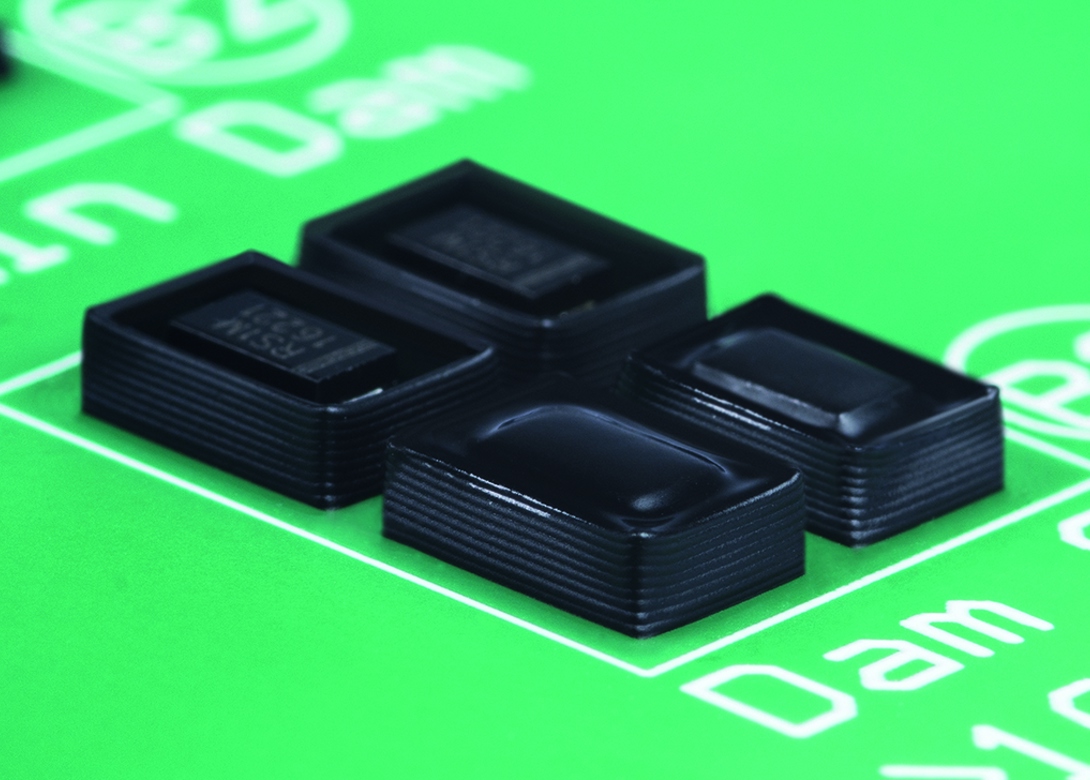
Another solution to increasingly miniaturised designs, in combination with high reliability requirements, are dam encapsulants. They allow very thin and high walls to be formed, which makes them ideally suited for automotive and industrial applications.
This is possible thanks to smaller sized fillers than those used in previous dam products, allowing the encapsulants to be applied through needles with a minimal diameter of 250μm. Thanks to an exceptionally high viscosity of up to 160,000 MPa, the adhesive additionally provides high flow resistance. This allows for an aspect ratio of 2.5 – i.e the height of an adhesive bead can be twice its width without the bead collapsing.
These characteristics make the easy to handle adhesive perfectly suited for the finest structures such as high separating walls between sensors, which require little width. Stacking of bead layers, known as ‘dam stacking’, is possible without curing in between and simplifies the production process.
These non-slump dam products also provide excellent resistance to acids, oils, and other aggressive media, and exhibit only low water absorption. They are suitable for use in a temperature environment of up to 200°C. The compression shear strength achieved on FR4 at room temperature is 49 MPa. This value changes very little and even after 500 hours of storage at 200°C, it is still at 43 MPa.
A low coefficient of thermal expansion (CTE) of 24ppm/K in combination with a high glass transition temperature of 180°C keeps warping at a very low level over a large temperature range, thus minimising stress to the package.
The dam products are available either as purely heat curing adhesives or, for even more flow resistance, as a dual curing version. The curing process can be controlled flexibly, choosing variable conditions in terms of time and temperature, for instance 20 minutes at 150°C or 90 minutes at 125°C. Since the adhesive does not flow, the aspect ratio remains unchanged. Therefore the height of the adhesive bead does not change through the heat curing process.
Even in applications that require maximum reliability, cost-effective production plays an increasingly important role. Both chip production and further chip processing are experiencing a strong trend towards rationalisation, for example in the field of chip encapsulation. This trend sees more and more manufacturers placing a large number of identical components on a PCB, which are then fully encapsulated and finally separated into individual encapsulated components. Another method applied is complete encapsulation of fully equipped PCBs instead of using housings to protect the circuit boards from environmental influences.
Large area encapsulation shortens process times significantly and holds great savings potential. However, this approach has often reached its limits in practice. In applications subject to high chemical and thermal stress, large area encapsulation has previously caused warpage of the PCB during curing. This effect caused tensions within the components and made saw singulation difficult. Such a warpage is the result of thermal mismatch between PCBs (10ppm/K – 20ppm/K) and encapsulants (usually more than 20ppm/K).
To address this issue, optimised encapsulants have been developed for high reliability applications, featuring a particularly low CTE value of 11ppm/K. This minimises warpage and makes the encapsulants perfect for efficient large area chip encapsulation. They are also available in fluorescent modifications allowing the application pattern and the full coverage of all components to be detected prior to adhesive curing.
The upper temperature limit of these products is currently 165°C, with excellent resistance to media and humidity. In addition, they offer excellent flow properties even without substrate heating and enable a ‘dam & fill’ process. These encapsulants also allow the curing parameters to be set variably. Rapid curing is possible within up to 20 minutes at 150°C, or the user can choose a low curing temperature of 100°C for one component products, or of 125°C for two component products. Even components that are more sensitive to temperature can thus cure reliably.
High-end encapsulants and potting compounds play a decisive role in protecting sensitive electronic components, even under the most demanding environmental conditions. Thanks to numerous new developments, users are now able to meet the increasing requirements of power electronics and the growing demand for miniaturisation – improving manufacturing efficiency.


Having spent a decade in the fastener industry experiencing every facet – from steel mills, fastener manufacturers, wholesalers, distributors, as well as machinery builders and plating + coating companies, Claire has developed an in-depth knowledge of all things fasteners.
Alongside visiting numerous companies, exhibitions and conferences around the world, Claire has also interviewed high profile figures – focusing on key topics impacting the sector and making sure readers stay up to date with the latest developments within the industry.

Don't have an account? Sign Up
Signing up to Fastener + Fixing Magazine enables you to manage your account details.